
Why Impedance Matching is Important | ThinkRobotics.in
We know that in the PCB design, Impedance matching means that when the energy is transmitted, the load impedance must be equal to the Characteristic impedance of the transmission line.
Impedance matching in the transmission lines:
In a high-Frequency signal system, any cable or wire with a physical length more significant than the wavelength of a signal passing through this wire is called the transmission line. There are various transmission lines, such as coaxial cables, waveguides, microstrips, strip-lines, etc.
Whether it is about the digital or the analog signals, impedance matching between a source, the transmission line, and load is a must. The reason impedance matching is essential in the transmission line is to ensure that a 10V signal sent down the line is seen as a 10 V signal at the receiver end.
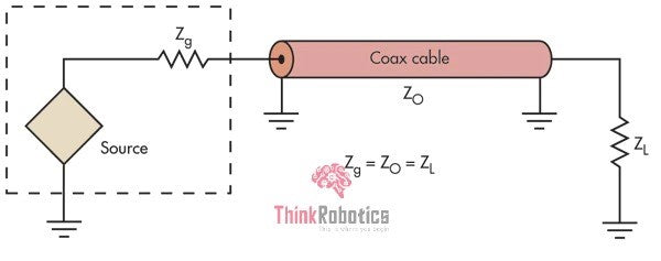
When we talk about impedance matching, we refer to setting the driver's impedance (source), the transmission lines, and the receiver to the same value. This is usually 50 Ohms for the single-ended transmission lines, although differential signaling standards may specify different impedance matching values.
All the transmission lines have a characteristic impedance (ZO), and that is a function of the transmission line's inductance and capacitance:

The presence of impedance discontinuities or mismatches reduces the amplitude and phase accuracy, also causing the temporal fidelity of measurements made with an electronic device.

The Measurement of the Match:
Reflection Co-efficient:
It can be defined as a specific parameter used to express the quality of a match. It is the ratio of the complex amplitude of the reflected wave to the incident wave's complex amplitude. Γ denotes it.
Γ = (ZL - Zo)/(ZL + Zo)
Where ZL is the load impedance
Zo is characteristics impedance, which is the impedance of the transmission line.
The coefficient has to be as small as possible. The ideal value is zero for the load impedance being equal to the characteristic impedance.
Case 1: say it is an ideal case with no impedance discontinuity that means both load and characteristics impedance are the same (ZL = ZO). Then, the coefficient (Γ) becomes zero (0).
Case 2: say the circuit at the load end becomes an open circuit that is ZL is infinite. Which is an invalid case.
Case 3: say the load impedance is zero; again, that makes for an invalid case.
Case 4: say ZL = 47 Ω; Zo = 20 Ω the, we have a valid case with a reflection coefficient of
Γ = 0.403 (it’s a ratio, so no units)
Voltage Standing Wave Ratio (VSWR):
It is about the impedance matching from the resulting standing wave’s point of view. It the ratio of the highest standing-wave amplitude to the lowest standing-wave amplitude. Standing waves represents the power that is not accepted by the load and reflected along the transmission line.
VSWR = (1 + | Γ |) / 1 - | Γ |)
VSWR is a critical parameter. An ideal case would be 1:1, denoting that the signal's peak amplitude is always the same (i.e., there is no standing wave). A ratio of 2:1 indicates that reflections have resulted in a standing wave with a maximum amplitude twice as large as its minimum amplitude.
There is also a ratio called Standing Wave Ratio (SWR), a generic description for both current and voltage standing waves. It is often the VSWR that is more widely used, as it is easier to detect and measure.
Importance of Impedance Matching:
Current digital and analog systems require impedance control and impedance matching due to the multitude of components necessitating fast rise time and low supply voltage and analog components that are running at higher frequencies.
- Failing of interconnects: As the frequency rises and the rise time reduces, your PCB is likely to fail if interconnects are not appropriately designed. Thus, it's highly necessary to have matched Impedances.
-
Preventing signal reflection: Whenever a traveling wave (be it electrical, optical, or acoustic) meets an impedance mismatch, there will be some signal reflection back towards the source. This is a fundamental property of wave physics, and it can't be denied.
 Fig 3: Reflections in The transmission line
-
Maximum power transfer: As it goes, maximum power can be transferred between two circuit elements when their impedances are matched. With oscillating signals, this is precisely due to suppressed reflections. Thus, matching impedances increases overall system efficiency. Some signaling standards do not rely on maximum power transfer and instead rely on high input impedance to sense a signal at the input.
 Fig 4: Max power is transferred when impedances of load and source match
 - Make the source/receiver impedance resistive. If the receiver has an inductive or capacitive impedance, it will show its transient response, which will differ from the ideal LC response seen in the transmission lines with resistive loads. Because the transmission line running at high frequency has a purely resistive impedance, the source and receiver impedances should also be made resistive to ensure impedance matching.
- High-speed digital circuits require very stable and controlled impedances because of its impact on the bit error rate and the potential for pulse distortion, reflection, and EMI.
Common Impedance Matching Method:
Series Terminal Matching:
Let us consider a case where the signal source impedance is lesser than the transmission line characteristic impedance. So, as reimbursement, a resistor R is connected in series between the source of the signal and the transmission line, such that the output impedance of the source end goes hand in hand with the characteristic impedance of the transmission line, and the signal reflected from the load end is suppressed.
Now, what is the value of R to be considered? The rule is that the sum of the matching resistor R-value and the output impedance (Zs) of the driver is equal to the transmission line's characteristic impedance.

This is a straightforward method. In the case of the CMOS and TTL drivers, in which the output impedance varies with the signal level, it is impossible to have an accurate matching resistor, which can only be assumed.
This method is prevalent and has a few perks- low power consumption, no additional DC load on the driver, no additional impedance between the signal and ground, and only one resistor.
Series Terminal Matching method is employed in the impedance matching of regular CMOS and TTL circuits and sampling of the USB signal.
Parallel Terminal Matching:
Suppose the impedance of the signal source is small. In that case, the load end's input impedance is matched with the characteristic impedance of the transmission line by increasing the parallel resistance R to eliminate the reflection at the load end itself. This can be implemented in two forms: single resistance parallel terminal matching and double resistance parallel terminal matching.

This method is simple and easy. The clear shortcoming is that the parallel connection brings DC power consumption. The single resistance mode's DC power consumption is related to the signal's duty cycle; the dual resistance mode is whether the signal is high or low. There is DC power consumption, but the current is less than half of the single resistor.
The Parallel Terminal Matching method is used in Stub Series Terminated Logic (SSTL) drivers such as DDR and DDR2. In single-resistance form, parallel to VTT. The parallel matching resistor of the DDR2 data signal is built in the chip for convenience.
High-speed serial data interface such as Transition Minimized Differential Signaling (TMDS). In the form of a single resistor, parallel to I/OVDD at the receiving device side, the single-ended impedance is 50 ohms (100 ohms between differential pairs).
With the rapid growth in the demand and the use of high-speed devices, PCB designers need to take account of many things; here, impedance control is of a high priority since it has a huge impact on signal integrity and the total operation of the board. By good analysis and study of the various factors responsible for the impedance mismatch and obtaining the knowledge of design practices that can lessen impedance issues, the PCB designers can create a perfectly engineered solution.

Impedance Matching Design in Optical Modules:
The optical modules offer an effective high-speed solution for a rising telecom market. Data rates as high as 155 Mbps to 6 Gbps and 10 Gbps are being developed. Transmitter optical sub-assemblies (TOSAs) and laser drivers may have different resistances in a given application, leading to impedance discontinuity. So, the reflection could be worse if an impedance transfer circuit is not used to absorb it. A poorly printed circuit board (PCB) layout can also be the source of additional uncertain noise and reflection. These problems can utterly affect output performance and destroy the results.
Even here, the reflection coefficient is used to know the degree of mismatch between the source impedance and the load impedance, with the same formula mentioned earlier, to determine the value of the reflection coefficient. At ΓL= 0, we have zero reflection and thus the most desired state.
In the receiver portion of the optical design, impedance matching is usually not a matter of concern. It is the transmission portion, which holds most of the reflection spots. For example, let us consider a case in which a reflection occurs at a point where the flex cable meets the TOSA (ROSA) elements. To reduce such reflections, some types of TOSAs integrate resistors to increase the TOSA impedance.
This additional resistor can be used with single-end type applications and differential types but preferred in the latter to avoid issues with common-mode noise and electromagnetic interference (EMI).
One potential problem is that the resistors consume current and heat the laser, which reduces the laser's overall efficiency. The driver must supply more modulation and bias current to maintain the extinction ratio (ER) and average optical power (PAV) setting because of the laser's higher temperature. Because of this, in recent years, most optical customers have transitioned their designs to use unmatched TOSAs.

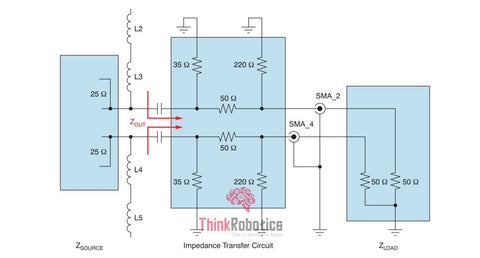
Impedance-Matched Systems
It is not always necessary to use an impedance transfer circuit. for example, the below fig. In the ONET8501V application presented here, the output impedance is 100-Ω differential; the transmission line is also 100 Ω, and the load is 100-Ω VCSEL TOSA. The resistance matches very well and produces minimum reflection.

Impedance Transfer for Mismatched Source and Load
This is the genuine case, where the use of the impedance transfer circuit minimizes the reflection by matching the source's impedances, the transmission line, and the destination. The eye diagram formation in the output, as shown in Fig.9, suggests the complete impedance match, which can also be absorbed.

Test Results:
Figures 12 and 13 show a few test results with the ONET1101L and NX8341TB TOSA (2 × 10-Ω internal resistors).
From these tests, we can see that the impedance transfer circuit works exceptionally well to improve the module reflection performance, although the circuit also increases the power consumption at the same time. For different TOSAs and power consumption requirements, we can adjust the resistors' values to achieve the best performance.


Sources:
- electronics-notes.com/articles/antennas-propagation/vswr-return-loss/what-is-vswr.php
- camptechii.com/the-importance-of-impedance-control-in-pcb-design-and-how-to-avoid-signal-integrity-problems/
- allaboutcircuits.com/textbook/radio-frequency-analysis-design/real-life-rf-signals/the-50-question-impedance-matching-in-rf-design/
- allpcb.com/sns/impedance-matching-in-high-speed-pcb-des_26232.html
- nwengineeringllc.com/article/why-impedance-matching-is-important-in-a-transmission-line.php
- resources.altium.com/p/why-impedance-matching-important-transmission-line
- electronicdesign.com/technologies/communications/article/21796367/back-to-basics-impedance-matching-part-1#:~:text=Transmission%20lines%20have%20a%20characteristic%20im
- ti.com/lit/an/slla311/slla311.pdf?ts=1600583673593&ref_url=https%253A%252F%252Fwww.google.com%252F
- bit.ly/2EstzZq
- bit.ly/2EstzZq
- bit.ly/2EstzZq
- bit.ly/2EstzZq
- bit.ly/2EstzZq
- bit.ly/2EstzZq
- images.app.goo.gl/TcXf2pZ5126qrFYS9
- images.app.goo.gl/YwfjBsfyh6vU7RH18
- images.app.goo.gl/YwfjBsfyh6vU7RH18
- images.app.goo.gl/6tcmUScHxqtZUDWK6
- images.app.goo.gl/dvygr5JMKS4tr26D7
- images.app.goo.gl/SRFzPhXvFT9ih4rk7
- images.app.goo.gl/8LbtYXWH8rSkQyHR8
Very informative and important to understand why we loose signal