ThinkRobotics PCB Designing Service

Introducing Highest Quality Service
In house | High Quality | Made in India
ThinkRobotics Quality Assurance
Certified Engineers | All Inclusive Service | Quick Quotation
Fast Delivery & Best in class support
Print PCBs up to 6 Layers | PCB Assembly Service | PCB Stencil development
Our Services

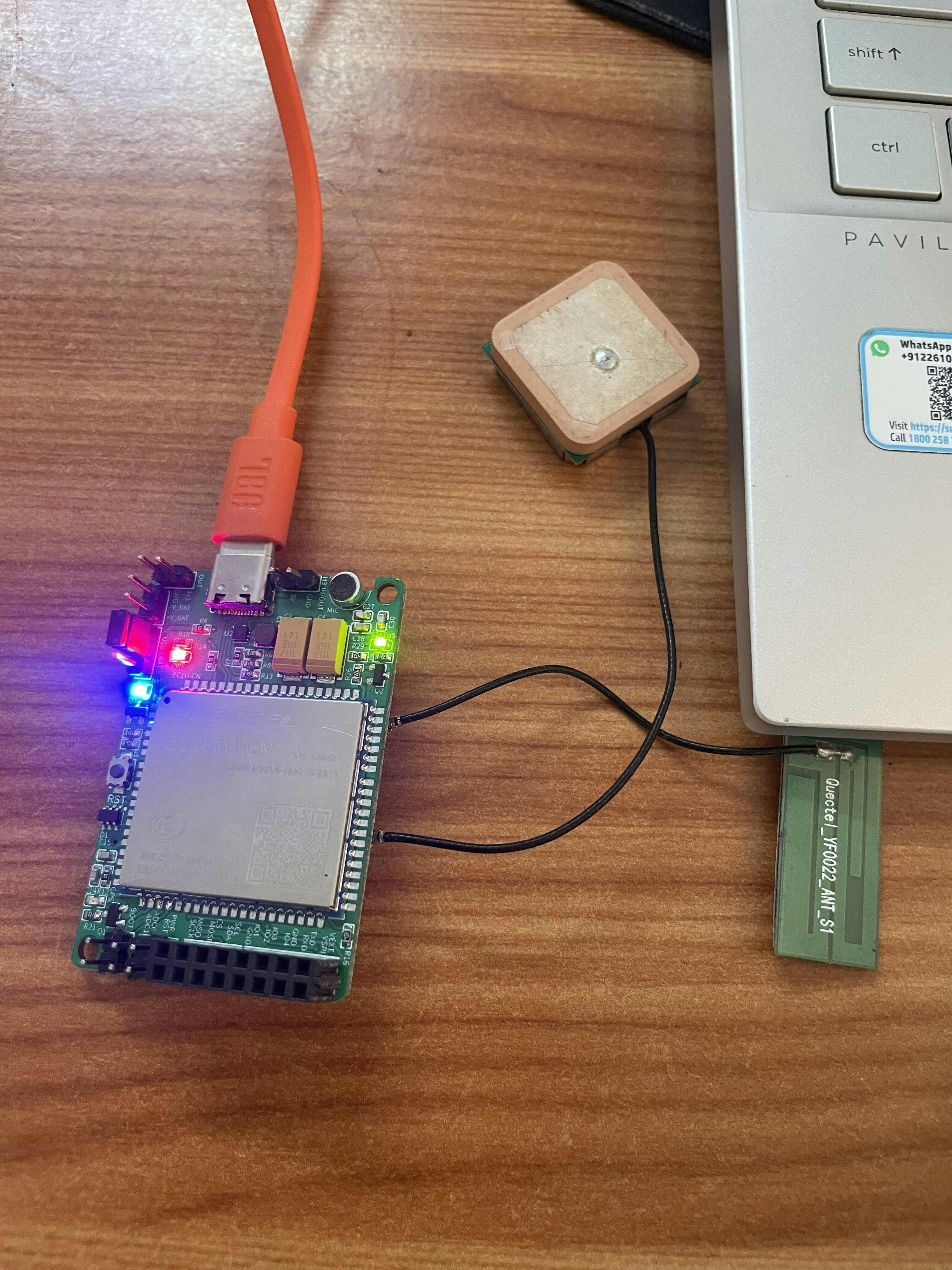
PCB Layout & Design
We use different PCB design software's to fulfill your needs: Altium Designer; Cadence OrCAD or Allegro; Eagle; which provides very high level PCB design files and output capabilities.

Electronics Development
Cooperating with professional electronics product design companies, we supply a comprehensive range of electronic design and development services to variety of international clients.

3D Printing
Work with our team of 3D printing and style experts to reinvent the way you produce jigs and fixtures, rapid prototypes, tooling, on-demand parts and low-volume production runs.

3D Modelling
Don't have a 3D Model? No problem! Our CAD team can get any project/idea into the the digital 3D world. You can design, build and prototype with the same team. Cutting down the turnaround time into half and saving you money and resources.
Box Build Service
Not only PCB assembly , but also a whole solution including mechanic assembly, software installation and supplied in packaging material. We control the whole process from procurement of mechanical parts to satisfy any customers expectations in terms of quality and reliability.

PCB Manufacturing
We don't just design your PCB but, also fabricate them for you! After the design phase we send the prototype within 14 days and after confirmation from our client, we move into mass production almost instantly.
Our Process
1
Receive Design Request
Design request form s filled by the client and is sent to our PCB team. After some initial communication the RFP and list of requirements are prepared. All communication henceforth are protected under an NDA.
2
Send Quotation & Begin Development
After deliberation, we send out a quote with 24 hours of first point of contact. The development starts after confirmation from the client. The design manager is assigned and single point of contact is maintained with the client throughout the process.
3
PoC & Prototype sent to Customer
The design of the PCB and layout is designed and tested internally. After first round of testing, the quality assurance, the design is transferred to the client for client side testing and possible design changes.
4
Proceed for Mass Fabrication
After testing, the PCB is moved for mass fabrication. Usually changes to the PCB shape is required for a snug fit in the outer enclosure of the product. After confirmation from client, contract is set in place and production starts.