
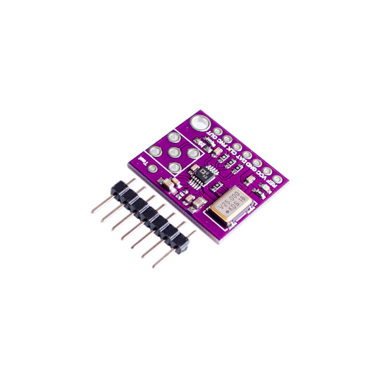


The AD9833 Function Generator Module is a frequency programmable sine, triangle and square wave generator with SPI interface.
FEATURES:
- 0-12.5MHz output frequency range
- 0.1Hz resolution
- 10-bit digital-to-analog output converter
- Sine, triangular and square waveform outputs
- Simple and complex modulation capability
- Phase control
- 3-wire SPI interface
- 3.3V and 5V logic compatible.
The AD9833 function generator can be used to provide various signals for electronic testing by serving as a function generator and it can be used in various sensing, actuation and time-domain reflectometry (TDR) applications such as for testing cables or for FSK or other keying application.
Powering the Module
The module can operate from 2.3 to 5.5V and so is compatible with both 3.3 and 5V MCUs.
Internally, the AD9833 contains a 2.5V regulator and operates at 2.5V. In the event that you want to operate the module at a Vcc voltage < 2.7V, the location on the board marked R1 which is normally open should be shorted so that VCC is connected directly to the CAP2.5V input which bypasses the internal regulator.
A red LED illuminates when power is applied to the module.
Waveform Output
The AD9833 can be programmed to output either a sine, triangular or square wave. When the module is first powered up, it automatically outputs a default 1kHz sine wave.
Sign Wave
The AD9833 creates sine waves by the use of a numerically controlled oscillator, phase modulator, sin look-up ROM and DAC.
The output DAC is a high impedance 10-bit current source DAC. A built-in 200 ohm load resistor converts the current to a 0.6Vp-p voltage output that swings between ground and about +0.6V. At frequencies above 1MHz, the signal amplitude starts decreasing.
Triangle Wave
When the triangle waveform is selected, the sin look-up ROM is bypassed and the output of the NCO is sent directly to the on-chip DAC which provides a 10-bit triangular output. The triangle wave output will also be approximately 0.6Vp-p up to 1MHz and then start to decrease at higher frequencies.
Square Wave
The square waveform is created by just sending the MSB (Most Significant Bit) of the DAC data to the output. Unlike the other two wave forms, the square wave output is a logic level and will swing the full range from ground to Vcc over most of its range.
Connecting to the output
The output of the AD9833 is available in 3 places. On the header pin marked ‘OUT‘, on the center pin of the unstuffed BNC connector location which is surrounded by 4 ground pins and at the pad marked ‘Tset‘.
The output of the module is not buffered. Depending on the applications, it may be desirable to add an op amp or similar buffer on the output to modify the levels and/or add drive capability. The output has a series resistor and capacitor location on the board. As-shipped, the resistor location is stuffed with a 0 ohm resistor. The larger C2 capacitor location next to it is unstuffed. If it is desired to AC couple the module, the 0 ohm resistor can be removed and a capacitor can be added to C2.
SPI Interface
The module has an easy to use 3-wire SPI interface that uses Data (SPI MOSI), Clock (SPI CLK) and Load (SPI SS) which is called FSYNC on the AD9833.
Module Assembly
This module comes with the header loose. This allows you to configure the module to meet your particular requirements such as which side of the board you want the header on or if you want to solder on wires to make the connections.
For use with breadboards, we put the headers on the bottom so that the module can plug directly into the breadboard.
If you are working with the module using an O’scope, you may find it handy to add a header pin to the Tset location for hooking up a scope probe. For some applications, such as building a little function generator, you may want to add a 5-pin BNC connector to the module to allow hooking up to BNC shielded cables
Module Connections
The connections to the module are fairly straightforward.
- Supply 3.3 or 5V power and ground from the MCU
- Connect the 3 SPI pins to the SPI pins on the MCU. Location of these pins will depend on which module you are using
- Hookup a scope to the output to see what the generator is doing
1 x 7 Header
- REF = 25MHz Reference clock from the on-board oscillator is output on this pin.
- VCC = Vcc power (2.3 to 5.5V)
- GND = Ground
- DAT = SPI Bus Data pin (MOSI)
- CLK = SPI Bus Clock pin
- FNC = SPI Bus Load pin (SS) (called FSYNC on the AD9833)
- OUT = Output of the function generator. Also available on center pin of BNC location and Tset
OUR EVALUATION RESULTS:
These modules have good build quality and generally work well, but don’t expect to run them up to the maximum 12.5MHz frequency spec of the AD9833. The AD9833 is a DDS (Direct Digital Synthesis) chip and as the output frequency approaches the clock rate, which is 25MHz in this case, the ability to reproduce the requested waveform starts to degrade.
Stability is good up to about 1MHz and then the waveform start to degrade as the frequencies increase from there. Depending on the output type, the signal holds together reasonably well up to about 5MHz. Refer to the O’scope pictures below to get an idea of the expected performance.
The frequency accuracy is good. On a sample basis we measured the following using the sine wave output.
- 100Hz measured 100.03Hz
- 1kHz measured 1.00001kHz
- 10kHz measured 10.0004kHz
- 100kHz measured 100.005kHz
- 1MHz measured 1.00005MHz
Below are some O’scope waveform captures showing typical performance of the three waveforms at several different frequencies. The measurements are taken at the BNC center pin location with a short ground probe contacting one of the BNC ground points.
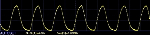
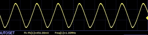
The first three show the sine wave output first at 1MHz with a p-p amplitude of 536mV, 5MHz where the amplitude has decreased to 216mV and the waveform is starting to show a little distortion and then at 9MHz where the amplitude is reduced further to 104mV and the waveform is starting to seriously deteriorate.
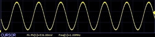
Sine Wave Output – 1MHz
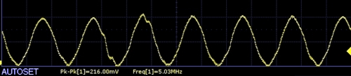
Sine Wave Output – 5 MHz
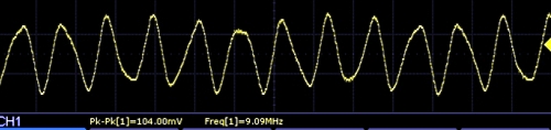
Sine Wave Output – 9MHz (showing waveform degradation)
These next three show the square wave output at 100kHz with an amplitude of 5.12V and then at 1MHz where the amplitude is still 5.12V but the edges are starting to show some roll-off and then at 5MHz where it is showing significant roll-off and amplitude has dipped slightly to 4.8V.
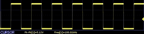
Square Wave Output – 100kHz
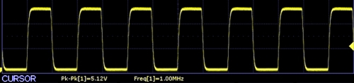
Square Wave Output – 1MHz
Square Wave Output – 5MHz
The next two shows the triangle wave output at 1kHz with an amplitude of 616mV and at 1MHz with an amplitude of 156mV.
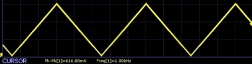
Triangle Wave Output – 1kHz
Triangle Wave Output – 1MHz
Getting A Look At The Output Of The Function Generator
This is not a trivial module to use due to the complexity of the output waveform. Having access to an O’scope is highly recommended in order to determine what the output is doing vs. what you think it should be doing. If you are working without an O’scope, a frequency counter can help determine at least the frequency of the output.
For experimenting purposes you can also feed the output of the generator into an analog input on an MCU. By reading the data at a fast rate and sending it to the Serial Plotter window it is possible to capture the waveform. For this to work reasonably well, the frequency needs to be kept low. In the example shown here, we are capturing a 10Hz sine wave output of the AD9833 on an Uno.
Here is a example of a simple program that can be used to capture the output. Connect the AD9833 module output which has been programmed to a low frequency waveform to the A0 analog input of the MCU. Download this program and then open the Serial Plotter Window to see the result. Make sure to set the Serial Plotter Window to 115200 baud rate.
/*  Read and Plot ADC Test Program

    Basic code to read from one of the analog port and send that data out
    to the Serial Plotter window to use as a budget O'Scope
*/
//===============================================================================
//  Initialization
//===============================================================================
void setup() {
  Serial.begin(115200);         // Set comm speed for serial monitor window
}
//===============================================================================
//  Main
//===============================================================================
void loop() {
  int adc_Reading = analogRead(A0);              // Read value from ADC
  float voltage = adc_Reading * (5.0 / 1023.0);  // Convert raw reading into a voltage
  Serial.println(voltage);                       // Send to Serial Plotter Window
}
The graph below shows the resulting Plotter Window output of the 10Hz sine wave.
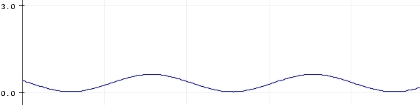
Serial Plotter Window – 10Hz Sine Wave Output of AD9833
If you have two Arduino boards, you can run this program on one and the program below on the other which allows you to control the AD9833 at the same time. If you have a single board, you can set the waveform using the software below and then load the ADC capture program to see the resulting output.
AD9833 Control Program
The program below uses the MD_AD9833 library which is available for download directly from the Arduino IDE.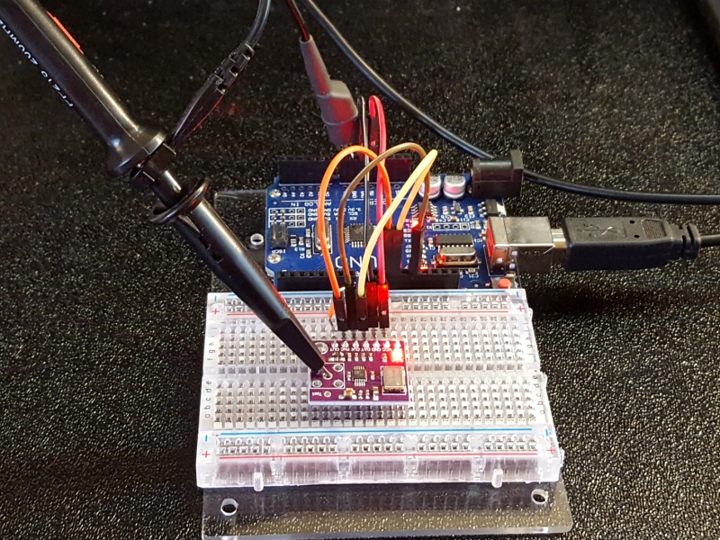
Connect 3.3V or 5V power, ground and SPI interface as shown below. SPI MISO is not used since this is a write only device. Be sure to update the SPI #define statements with the pins that your board uses for the SPI interface. A couple of the more common ones are shown below.
Uno: DATA pin 11, CLK pin 13, FSYNC pin 10
Mega 2560: DATA pin 51, CLK pin 52, FSYNC pin 53
The program allows you to select the type of waveform to output and to set the frequency of the output waveform. Once the library is downloaded, a sample program is available which provides more insight into the advanced uses of the module but the logic can be a bit tough to follow.
Once the program is downloaded and running, commands can be entered into the Serial Monitor Window. They can be entered either lower or upper case. Press enter to send the command to the MCU. Once the MCU receives the command, it will echo it back to the Serial Monitor Window to show that it got the command.
Valid Commands:
- F x to F xxxxxxxx = Sets the frequency of the output. Type ‘F’ plus the frequency you want, then hit enter
- S = Set to Sine wave output
- T = Set to Triangle wave output
- Q = Set to Square wave output
- O = Turns output off
- ? = Prints this command list
AD9833 Function Generator Module Test Program
/*MD_AD9833 Test Program
 *
  Exercises the AD9833 Function Generator Module
  Allows output waveform to be set to sine, triangle, square or off
  Allows frequency to be set to 1-12500000
  Uses standard SPI hardware pins for interface, in this case pins 10, 11, 13
*/
#include <MD_AD9833.h>
#include <SPI.h>

// Pins for SPI comm with the AD9833 IC on Uno
#define DATA  11	    // SPI Data/MOSI pin number.  Meg 2560 uses pin 51
#define CLK   13	    // SPI Clock pin number.  Mega 2560 uses pin 52
#define FSYNC 10	    // SPI Load/SS pin number.  Mega 2560 uses pin 53

MD_AD9833	AD(FSYNC);  // Hardware SPI

char readString[9];       // String array to hold frequency value
uint32_t freq_Value = 0;  // Frequency value to set
//===============================================================================
//  Initialization
//===============================================================================
void setup(void)
{
  AD.begin();
  Serial.begin(9600);                  // Initialize serial monitor
  PrintCmds();
}
//===============================================================================
//  Main
//===============================================================================
void loop(void)
{
  if (Serial.available()) DoSerial();  // Loop looking for something on serial port
}
//===============================================================================
//  Subroutine to handle characters typed via Serial Monitor Window
//===============================================================================
void DoSerial()
{
  MD_AD9833::mode_t mode;
  int index = 0;                    // index into string array

  char ch = toupper(Serial.read());  // Read the character and convert to upper case
  Serial.print(ch);                // Echo character to serial monitor to show we got it

  // Use Switch/Case statement to handle the different commands
  switch (ch) {
    case '?':   // Print commands
      PrintCmds();
      break;

    case 'F':   // Set output frequency
      delay(2);  // Give time for more characters to arrive.
      for (int i; i < 9; i++) readString[i] = ' '; // Clear string array
      while (Serial.available())  // While there is more chars coming in
      {
        char c = Serial.read();   // Read what we get and put into the string array
        readString[index] = c;
        index++;
        delay(2);
      }
      readString[index] = '\0'; // Append null to end of string array to make it a valid string

      freq_Value = strtoul(readString, NULL, 10);  // Try to convert string into unsigned long
      // We assume a 0 value is because of a non-valid input and ignore the command
      if (freq_Value != 0) {
        if (freq_Value > 12500000) freq_Value = 12500000;     // Cap value at theoretical max
        Serial.println(freq_Value);        // Echo what we end up with to confirm we got it
        AD.setFrequency(0, freq_Value);
      }
      break;

    case 'S':   // Set waveform type to SINE
      mode = MD_AD9833::MODE_SINE;
      AD.setMode(mode);
      break;

    case 'T':   // Set waveform type to TRIANGLE
      mode = MD_AD9833::MODE_TRIANGLE;
      AD.setMode(mode);
      break;

    case 'Q':   // Set waveform type to SQUARE
      mode = MD_AD9833::MODE_SQUARE1;
      AD.setMode(mode);
      break;

    case 'O':   // Set output OFF
      mode = MD_AD9833::MODE_OFF;
      AD.setMode(mode);
      break;
  }
}
//===============================================================================
//  Subroutine to print the command set to the Serial Monitor Window.
//===============================================================================
void PrintCmds()
{
  Serial.println("Enter command:");    // Printout commands
  Serial.println("F xxxxx = Set frequency in Hz");
  Serial.println("S = Set SINE waveform output");
  Serial.println("T = Set TRIANGLE waveform output");
  Serial.println("Q = Set SQUARE waveform output");
  Serial.println("O = Turn OFF output");
  Serial.println("? = Show commands");
}
BEFORE THEY ARE SHIPPED, THESE MODULES ARE:
- Sample inspected and functionality verified per incoming shipment.
Notes:
- None
TECHNICAL SPECIFICATIONS
| Operational Ratings | ||
| Vcc | Range | 2.3 – 5.5V (3.3 or 5V typical) |
| Frequency | Specified Range | 0 – 12.5MHz |
| Waveforms | Sine, Triangular, Square | |
| VOut | Square Wave (MSB bit) | 0 – Vcc |
| VOut | DAC Minimum Output Voltage | 38mV |
| DAC Maximum Output Voltage | 650mV | |
| Resolution | Output DAC | 10-bits |
| Dimensions | L x W (PCB) | 24 x 20mm (1 x 0.78″) |
| Datasheets | Analog Devices | AD9833 |